Ethernet: Past, Present and Future, Part 2

The first article of this series took a look at the humble beginnings of Ethernet and how it began to accommodate advances in network technology. This second installment looks at how FPGA technology has evolved to support FPGA-based network acceleration cards (NACs). This advancement enables the design of very flexible hardware platforms, supporting a broad range of existing and new use cases, all with an extended lifetime.
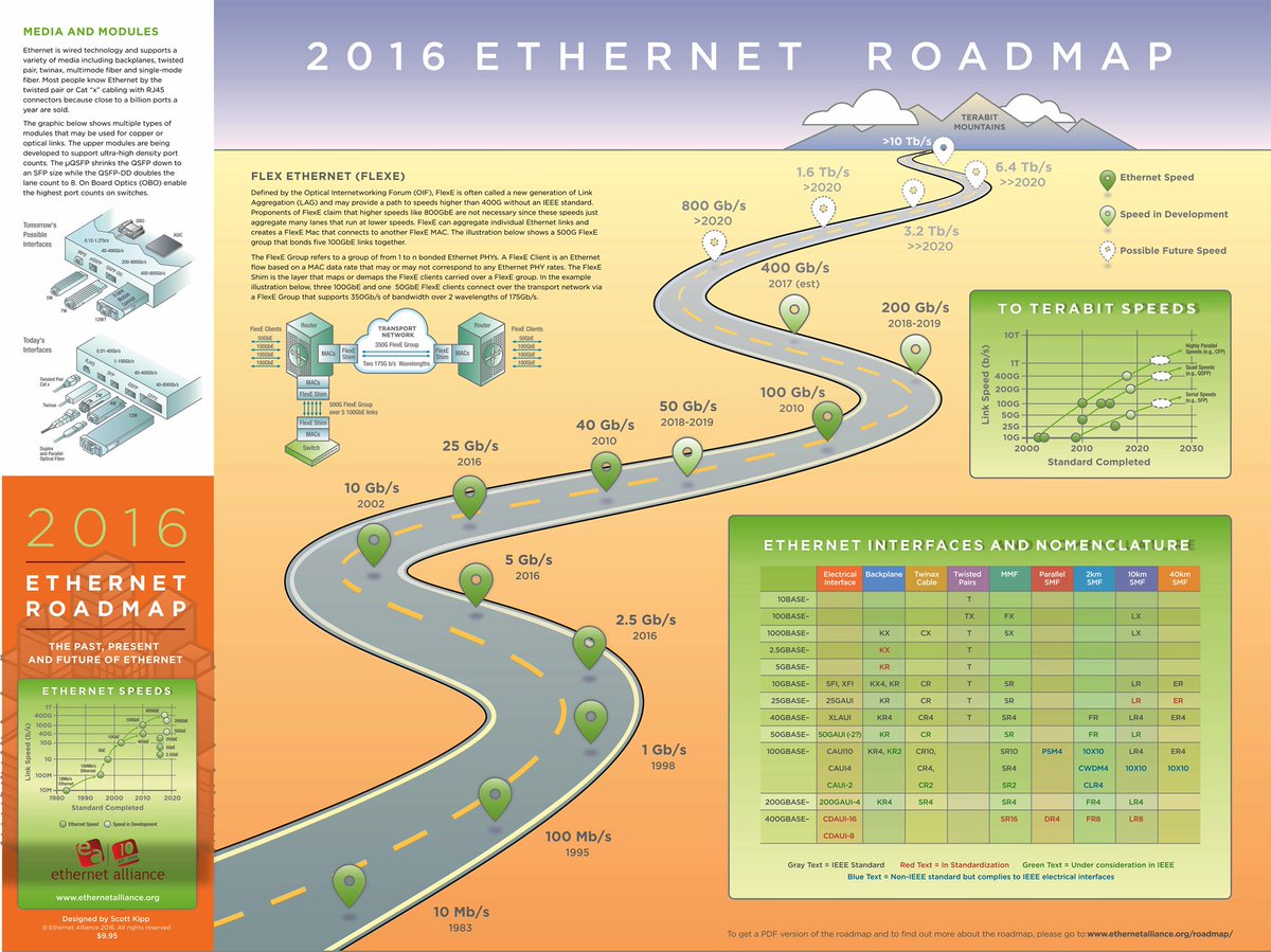
A good place to start is to understand what is possible from a future-proof FPGA based NAC. An NAC hardware platform based on FPGA and designed to be future-proof should support:
- Ethernet link speeds and types available currently and in the near future, through attractive front port connectivity
- Different FPGA size configuration, providing the customer with the right cost/feature ratio options, enabling competitive product offerings (see Figure 1)

In the past, FPGA-based NACs have deployed the so-called PHY devices in the data path between the FPGA and the Ethernet front port. The discreet silicon PHY device handles the physical layers of the Ethernet protocol stack.
To achieve the highest port rates, the PHY device has usually been needed because it added functionality not available in current FPGA technology. For other port rates the PHY device represents an attractive compromise between cost and NAC features.
The main reasons for implementing PHY devices are:
- Logical resource constraints in the FPGA
- Minimizing BOM cost
- FPGA transceiver speed limitations
The PHY device compensates nicely for the above-referenced FPGA limitations – but it typically restricts the design in the number of supported Ethernet link speeds and potential types.
Though 25G transceiver technology was introduced in the 28nm FPGA process node, it was only made available in a few high-end device options, available at a substantial cost, compared to the mainstream device options. For good reasons, besides the cost factor, the initial 100G FPGA-based NAC offerings deployed PHY devices implementing the required so-called gearbox functionality and optional error correction functionality. As with the previous PHY application, the gearbox PHY restricts these designs in the number of supported Ethernet link speeds to just 100G.
With the introduction of the latest 20nm FPGA families from Xilinx and Intel (former Altera), the FPGA technology is on par with the current and near-term future Ethernet link speeds, rendering obsolete the need for the PHY companion devices.

A PHY-less, FPGA-based NAC design offers the following obvious benefits from a multi-link speed customer perspective:
- Ability to introduce multi-link speed product variants, eventually handling all major link speeds and types, on the same ports, through dynamic reconfiguration.
- Restriction of the required knowledge base to one platform
- Ability to source many different product variants with the same NAC part number
- Reducing the number of required hardware qualification resources
- Collecting volume on one or few NAC part numbers, pleasing logistics and pricing
The last of this three-part series will examine the front port connectivity options that maximize the market value of the above-referenced future-proof FPGA platform. We will explore three elements: physical form factor, supported link types and supported link speeds.

